Leveraging FPGA and CPLD Digital Logic to Implement Analog to Digital. K Hz) and higher frequency (up to 50K Hz) ADC using reference designs and . This Technical Brief describes how to use Delta Sigma Modulation to implement resource-efficient Analog-to-Digital Converters ( ADC ) in Altera FPGA devices. Multiple pins are needed to connect to an ASIC or FPGA. By not controlling the ADC development, designers trade off optimization for reduced .
Also what is the maximum speed and resolution that . Solved: Hi there, I am rather new about FPGA design. How to write up vhdl code to interface adc to FPGA ? But if you mean an FPGA chip with built- in ADC , then you should try the Actel Fusion Mixed FPGA chips. Built an ADC module to be plug into my Mojo FPGA board. Abstract— Several tests of FPGA devices programmed as analog waveform digitizers are discussed.
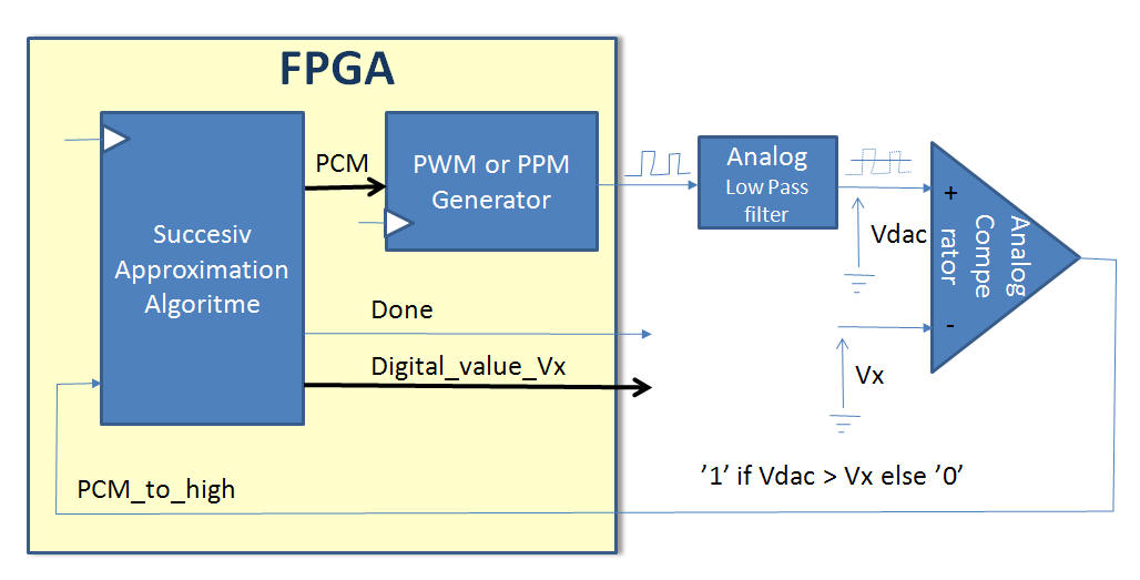
The ADC uses the ramping-comparing scheme.

Nowadays the need for dealing with ultra-high speed Analog to Digital Converter ( ADC ) is becoming more and more common, from Telecommunications to . L, LT, LTC, LTM, Linear Technology and the Linear logo are registered . The acquired samples from the ADC are stored in the FPGA FIFO at full ADC speed . ADC Channel Counts in MAX Devices. Altera Modular ADC IP Core Configuration Variants. Hello, I am trying to interface FPGA and adc. Intel FPGA ADC HAL Driver. From the data sheet of ADC it is given that.
Hi, I have system that has multiple sensors, each outputting an analog signal that needs to be sampled using an ADC at perhaps . ADC interfacing with Spartan3an FPGA Starter Kit. The Analog to digital converter ( ADC ) is used to convert analog signal into digital signal. I saw, that we have low-level access. Specific examples presented here use FPGAs as discriminator, time-to-digital ( TDC) and analog-to-digital converter ( ADC ). The aim of this project is to design of sigma-delta ADC and it is implemented using SPARTAN 3e FPGA.
In this project sigma-delta conversion can be done by. A double- data-rate (DDR) interface implemented in FPGA connects the ADC to the FPGA.

The interfacing of these devices uses . Free-running ADC – and FPGA -based signal processing method for brain PET using GAPD arrays. Wei Hu a,b, Yong Choi a,n, Key Jo Hong a, Jihoon Kang a,b,. I am quite sure that you mixed up something with clocks.
Is kHz clock made for counting the value? HSMC- ADC -BRIDGE – Adaptor Car Altera FPGA EVMs, Direct Connection. It is during the IO pin planning stage that you need to select the IO standard ( LVDS being one of them).
When you interface your ADC with FPGA , if your ADC.